
AMD's Carrizo APU will redefine the mainstream notebook (updated)
*Updated on 12th June* - We've now added far more details, photos and videos to the originally published article on 3rd June.
First announced at AMD's Future of Compute event in Singapore late last year, and further teased with some of Carrizo's inner workings earlier last quarter, Carrizo - AMD's 6th generation APU - will finally be available by end of the month.
Aside from improved performance that can be expected from a more advanced DirectX 12 capable third-generation GCN graphics core based graphics engine, its all new Excavator core is highly optimized for power efficiency and is the first APU to integrate the Southbridge chipset functionality within the same APU die. This means Carrizo APU based systems are much more streamlined with better power control as there's less out-of-chip interdependency to manage.
Today at AMD's Tech Day in Computex 2015, AMD has showcased and shared with top media around the world of Carrizo's capabilities and the market space it will address. First and foremost, AMD's Carrizo will first make its appearance in the mobile space - specifically notebooks of all sorts. As such, you and I won't be able to get one off your PC components store, but you'll have to wait for the big notebook vendors to retail their mobile computing products into the retail channel. AMD was positive that by end of June, notebooks featuring Carrizo will be made available. To prove that point, check out the showcase of a number of tier-1 notebooks that are powered by Carrizo at their press conference in Computex.
The case for Carrizo and its target market
It's 2015 and while we don't yet have flying cars or a hover board that goes anywhere, you most certainly have a fitness tracker to keep a close watch of your activity trends, a couple of mobile phones to cater to your personal and work spheres or simply because you want to be seen with a device that best matches your style for the day, a smartwatch to glance at notifications, and probably a tablet for extended reading or media consumption while you're on the move.

Even with the rise of gadget distraction, it's more than likely that a computing device such as a desktop or notebook is used to sync and manage all these mobility gadgets and rely upon for any serious tasks such as content creation, media management, enjoying content on a big screen and of course gaming. The computer is no less relevant today than it was decades ago, apart from its shifting form factor. Falling prices and improved capabilities of notebooks made these mobile computers a more versatile and preferred workstation of choice for a wide variety of folks.
Brand owners and reviewers like ourselves love to showcase the expensive tech toys outfitted with the top-end specs and features. However, more likely than not, people are going to buy a mainstream variant. The reality is that the mainstream segment is where the volume shipments happen, and by a far larger margin. According to IDC, nearly 40% of all notebooks shipped in 2015 belong in this segment - the US$400 to US$700 bracket (~ S$500 to S$1000). That alone amounts to 63 million notebooks and that's a huge figure.

However, a large portion of notebooks in general is powered by Intel and while we have to give them credit in enabling the market to push new form factors and frontiers, they are also often on the expensive end. The mainstream market is focused on price and functionality and it's an area that Intel usually doesn't deliver as well when compared to AMD's solutions at a similar price point - especially within the sensitive US$400 to US$700 price bracket.
Consider that the main usage trends for computing devices these days are to create and manage content, stream videos and indulge in online gaming - tasks that all notebooks can partake - the exact question is how satisfying is your quality of experience? Note that these tasks are increasingly being accelerated by relying on the GPU but that's one area where as much as Intel perseveres, its integrated GPU leaves much to be desired. Taking a page off desktop processors where we've compared AMD's A10-7850 Kaveri APU against a variety of Intel processors last year, the Kaveri APU shows its chops for GPU intensive tasks.
This is the main reason why you often see Intel based notebooks boasting of a discrete GPU to make up for the poor showing of the integrated GPU. This adds to the cost, complexity and form factor of a notebook. When not implemented properly, such as a notebook boasting an NVIDIA discrete GPU but lacking NVIDIA Optimus technology, your power consumption skyrockets due to inefficient use of the discrete GPU, thus affecting battery life of the notebook.
Having identified the target market, this is where AMD's new Carrizo APU hopes to deliver enhanced user experiences and capabilities to a price sensitive mainstream segment with better battery life, top notch video, gaming and GPU compute capabilities than what the competition offers and improve over what Kaveri did for notebooks last year.
Carrizo mobile processor line-up and availability

As the image above depicts, AMD is kick starting the Carrizo line-up with 3 key models, one in each class of APUs - A8-8600P, A10-8700P and the FX-8800P. As you can guess by now, all Carrizo class APUs will have an 8xxx processor numbering schema. All three models have a ‘quad-core’ CPU portion, but only the FX-8800P had a Radeon R7 class GPU with eight Compute Units (CUs). The other two models have Radeon R6 class graphics with lower clocks speeds and only six CUs.
More APUs models to be made available in the future, but this is Carrizo’s first salvo. As pointed out earlier, AMD expects Carrizo equipped notebooks to hit retail by end of the month or just after and here’s what the notebook line-up looks like from actual partner vendors – all of which are big name players, so that's encouraging.
If you’re expecting how the performance figures stack up between these three APUs and that from Kaveri, we’ll reveal some of that later in this article as we deep dive and showcase all of the changes AMD has made underneath to bring about their next generation mobile platform for the masses.
AMD expects their top FX-class processor to compete favorably against a Core i5-5200U processor based notebooks from Intel – a popular chip for several mid-range notebooks.
Performance Preview of a Reference Carrizo Notebook

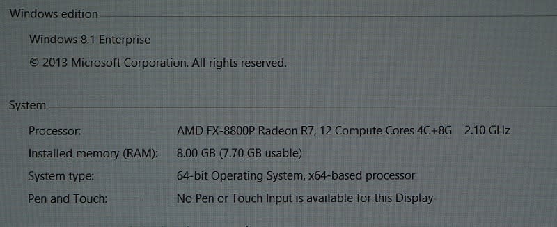
Since the actual retailer notebooks won’t actually be out until perhaps next month, we were provided with an opportunity to interact with a Carrizo powered reference notebook. It might not look like much, but it has got it where it counts the most. The reference machine is outfitted with the top model APU, the FX-8800P. It was our good luck that the notebook wasn’t really fastened, so we got a quick look inside of it too:-
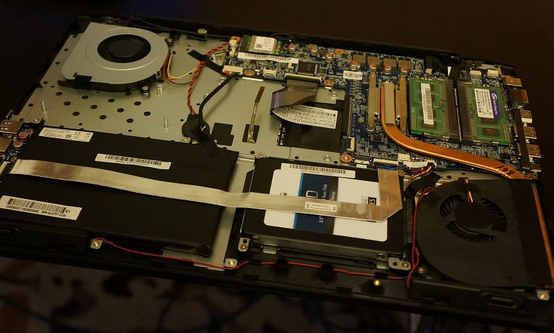
Note the really compact area of the PCB that houses the brains and logic of the entire system while the rest of the machine is home to cooling fans, battery and storage devices. Such is the advantage of System on a Chip (SoC) solution, which is the new Carrizo and that really simplifies much of the innards within the notebook.
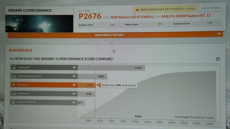
Here are some preview results to showcase where the FX-8800P stands, but we’ll have to wait for the retail edition notebooks to really figure out if the meet the reference standard or even better it:-


What you’ve seen is just a snapshot of the Carrizo APU’s capabilities but there’s much more to it than just benchmark numbers. We deep dive into the architecture of the APU and share more of its capabilities and the experience you will get out of it on the following page, so read on!
Deep diving into Carrizo

Carrizo is now an SoC part just like Beema and Mullins with all Southbridge chipset functionality now on-die with the APU. It will also inherit the AMD Platform Security Processor (PSP) that's based off an ARM Cortex A5 with ARM TrustZone technology for enterprise-class security and new power management techniques like Skin Temperature Aware Power Management (STAPM) and Intelligent Boost Control. You can read more about all these technologies in our AMD Mullins Preview article for more details.
While that might not sound like much of an advancement, it is in fact a big achievement as Carrizo is the first performance class APU that's designed to be an SoC and what's more, AMD managed to deliver all these extra functions with a die size comparable to that of Kaveri which didn't have any of these. And yes, there's no die-shrink - it's still using the same 28nm process technology as used in their last generation too.
So how does Carrizo achieve smoother, snappier, more efficient performance than its predecessor with lower power draw and yet adds more functionality without adopting a shrink in process technology or an increase in die size that would affect cost? Traditionally, you only get these advantages by adopting the next manufacturing process technology. However, AMD has been evaluating its partner's (TSMC) next process node for some time now and has concluded that TSMC's 20nm node isn't suitable for high performance parts and was more suited to power efficient low wattage processors like those used in phones.
Joe Macri, an AMD corporate fellow and CVP product CTO, said squarely that AMD didn't have much of a choice as their next viable hop was for 14 or 16nm FinFET transistor architecture which was still some time out before they can harness it. In the meantime, AMD's engineers had to innovate, or else they wouldn't have had a Carrizo to launch today.
The new Excavator Core

AMD's engineers had to try something new, even methodologies that go against the grain. They took a chance to try a different choice of transistor libraries for the CPU core. Kaveri's "Steamroller" core used a high performance library implementation, but Carrizo's "Excavator" core adopted high density library design. This allowed AMD to achieve a 23% die area reduction and lower power - all while still on the 28nm technology node. The downside to using the high density transistor library is that it’s difficult to ramp up clock speeds to a high level, but since it’s for low power processor parts - 15w to 35w TDP - the choice to adopt high density libraries vs. high performance libraries paid off for Carrizo.
That's a massive savings of die space which went into putting in more functionality within the die, such as the FCH chip (Southbridge functionality), AMD's PSP and a far beefier Unified Video Decoder (UVD) engine. This was how AMD managed to integrate so much functionality into a premium performance APU part.
That's not all; the Excavator cores were also enhanced to the point that it's able to churn out 4 to 15% more instructions per clock cycle than the predecessor. Here are some of the key improvements:-
L1 cache size has been doubled, along with prefetch enhancements and better latency. There's also reduced power consumption of up to 2x through better clock gating and other array changes.
Better branch prediction with a 50% increase in Branch Target Buffer Size (formerly 512 entries, it's not 768 entries).
New instructions support - AVX2, MOVBE, SMEP and BMI1/2. Software compiled to recognize these instruction hooks will accelerate processing and reduce power and time required.
Support for Modern Standby low power modes - greatly improves standby speeds.
Probably the only key specification that had to be compromised was the size of the L2 cache - it's now 2MB, whereas Kaveri had 4MB. To compensate for the reduction in L2, AMD consciously improved the efficiency of the core and bolstered the L1 cache capabilities as outlined above. To showcase the capability of the new Excavator core, AMD has this performance slide to compare against its predecessor's Steamroller core:-

Vastly improved UVD engine with 4K videos and hardware HEVC decode support
With a radically improved Excavator CPU core, AMD was able to achieve unprecedented die area savings based on the same manufacturing process node. AMD then decided to bolster other areas of its APUs and one key agenda is to improve video playback capabilities for current and next generation content.
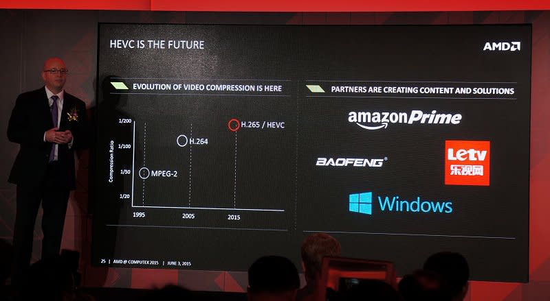
In all honesty, the universal video decoder (UVD) block of AMD's APUs is robust enough for today's needs, but AMD is looking forward and has recognized that smooth HEVC / H.265 decoding is necessary when tackling next generation video content. Known as High Efficiency Video Codec (HEVC), this requires more horsepower to process, but it can deliver higher quality videos than H.264 at any bitrate and at a smaller footprint. Shown in the above photo, content providers are already gearing up for this new codec to deliver either better quality videos or stream lesser data over the internet while still preserving the same video quality.
As such, HEVC / H.265 is fast becoming the next important video codec standard of choice, especially if you were to consider the even more processor intensive and data hungry 4K videos. Last year when the Kaveri APU debuted, it had software support for HEVC / H.265 playback, but it wasn't hardware accelerated. Even so, the APU was somewhat capable of tackling videos encoded in this format, though it comes at high CPU utilization and it may stutter occasionally.
On Carrizo, AMD equipped it with its new sixth generation UVD block and it is now far more powerful than ever. The UVD 6 now occupies a much bigger silicon footprint than its predecessors with four times the bandwidth processing capability to deal with 4K video content fluidly. As a byproduct of this new design, it actually helps to speed up processing 1080p content and allows the UVD engine to go to sleep faster as well as DRAM to lower power state, thus enabling power savings for most daily content viewed. According to AMD's testing, this aspect alone adds half an hour extra playback time.
UVD 6 also adds native decode acceleration for HEVC / H.265, native 4K H.264 content and 4K MJPEG along with everything else that its predecessors supported (such as VC-1, WMV, MPEG-2, MV, MPEG-4, DivX and more). Out of these, you might question, why 4K MJPEG? According to AMD executives, it seems like MJPEG is the format of choice supported by cheap web cameras installed on many notebooks. It won't be long before we see 4K-resolution capable web cameras and AMD is looking ahead to support 4K MJPEG in anticipation - with hardware acceleration to ensure there's no high overhead to the APU and the system in general.
So with is AMD expecting you to experience with the new and improved UVD 6? Uninterrupted smooth video playback with full CPU offload for 4K video content at 60fps. To prove that, we've personally experienced a reference AMD notebook using AMD's top Carrizo APU against a commercially available HP notebook equipped with Broadwell class mobile processor - Intel Core i5-5200U - with all other specs kept as equal as possible. The results are clearly visible:-
To sum the video, AMD's Carrizo APU leaves the competition in the dust. But performance isn't the only superlative they've achieved out of the UVD 6. We've also pointed out on the efficiency of processing that gets the processing blocks go to sleep sooner and thus save on energy, which in turn translates to a long video playback period.
AMD also went ahead to identify a GPU routine within the video playback pipeline that consumes power inefficiently. Video scaling and image processing are traditionally handled by the GPU but AMD added a new Underlay Pipe and additional circuitry to implement those functions directly within the display control engine. Cutting the GPU out of the video playback routine completely boosted the power savings achieved during this common task as AMD attests:-

Summing up, on Carrizo, you not only get vastly better video throughput performance, but it's also implemented in an efficient manner that you actually save power over a similar routine executed on Kaveri. AMD estimates an over 50% power savings for a 1080p video playback considering that there's no external FCH, the CPU core has been made more power efficient and the UVD too operates in a more streamlined manner than its predecessors, thus adding on to the savings achievable. In AMD's internal testing, an AMD FX-8800P Carrizo APU (15W) system put up against an FX-7600 (35W) system using the same 50Whr battery lasted over 8 hours watching a H.264 encoded 1080p video as opposed to the older Kaveri at just over 3 hours.

Carrizo's Graphics Core

AMD outfits their APUs with the latest graphics technologies possible to give them maximum features and performance capabilities possible out of integrated GPUs. While the number of GCN compute units (CU) possible within the Carrizo has stayed put at up to 8 CUs just like Kaveri before it (using a variation of the Hawaii core), AMD had adopted the 3rd generation GCN architecture that was utilized on AMD Tonga and later GPUs (sometimes referred to as GCN 1.2). This brings with it three main advantages over the previous GCN variant:-
An updated instruction set architecture (ISA) for improved compute and HSA performance.
Improved tessellation and geometry processing capability due to improved vertex reuse and distribution that tackles processing throughput of smaller triangles.
Lossless delta color compression that reduces memory bandwidth requirements and improves performance (especially in higher resolutions). Compared to the previous generation, this alone gives the Carrizo APU a 5 to 7% performance improvement.
Outside of the core GCN architecture, AMD added 16-bit float instruction support to better tackle video workloads that tend to utilize it. There's a also an upgraded high quality display scaler engine with 3 upgraded display controllers to tackle 4K display output needs since 4K monitors are everywhere and is within comfortable reach for most users who need the extra workspace provided by these high resolution displays.
Energy efficiency of the graphics core is crucial to optimize how high or low it can throttle up and down – not only in the graphics frequency department, but also the number of CUs in operation. Unlike past APU designs, Carrizo is the first to have a dedicated graphics voltage plane- something that should have been present from the start of APU designs. With independent voltage rails for CPU and GPU components within the core, energy consumption will be more optimally used as required by the application type instead of inefficient power consumption from applying a standard voltage across the entire APU and hitting the TDP wall sooner. This actually helps Carrizo unleash up to 33% more CUs than Kaveri (depending on the power profile it is operating), because Kaveri was known to have only been able to use up to six of its CUs when the APU was at high workloads and that’s not great if the task at hand needed more GPU horsepower.

Another piece to the power efficient graphics core is that Carrizo natively optimized for a lower power operation with a high density power design as opposed to a high performance design. There's even per-core power gating embedded for even more efficient power utilization. The net result is that Carrizo is optimized for a 15W TDP as opposed to Kaveri at 35W and it has increased frequency scaling for even more performance. As such, the APU is now a lot more capable at low TDP with up to 18% leakage reduction.
According to AMD, Carrizo is 65% faster in 3DMark11 over Carrizo. While that may not sound like an accurate measure of performance with such an old benchmark, here’s how Carrizo stands against Kaveri in popular online games:-

Last but not least, just like what we've shared of Godavari and Kaveri having FreeSync, VSR and DirectX 12 support, it goes without saying that Carrizo supports all of these as well. It will be most interesting to see how Carrizo powered notebooks equipped with a discrete GPU to take advantage of split frame rendering or also known as asymmetric rendering to pump up performance even further. Perhaps we'll get to see more of such systems next quarter.
First True HSA 1.0 Processor
A big deal about Carrizo is that it’s the first true Heterogeneous Systems Architecture (HSA) 1.0 compliant processor. While Kaveri allowed the CPU and GPU cores to have universal memory access and addressing space, along with executing compatible instruction in either the GPU or GPU cores, it hadn’t yet achieved the last stage of a true HSA compliant processor – it lacked support for graphics context switching to truly provide a level of quality of service (QoS). Carrizo delivers this with Wavefront and Compute task pre-emption and context switching to improve work scheduling efficiency along with HSA QoS scheduling support.

Other HSA acceleration features include the addition of Address Translation Cache (ATC) to improve virtual memory address translation throughput for data shared between CPU and GPU, and full hardware cache coherence at maximum DRAM bandwidth.
These four aspects not only ensure a HSA 1.0 compliant processor was achieved on Carrizo, but also one that can help realize HSA acceleration effectively. Here's a clip from AMD to show off it's compute performance utilizing all available computing cores:-
Closing Remarks
How much ever greatness AMD’s engineers have achieved from a technological standpoint to pull a Carrizo out of the Kaveri they had previously, putting aside all the tech talk, what we truly expect out of this APU is a seriously capable multimedia and mainstream gaming notebook machine for just over S$1,000. It’s simple market metrics.
If you scale the price any higher, AMD’s partners would have to compete with the various other offerings that Intel puts out from sexier, ultrathin, compact and portable machines to chunkier machines that offer discrete mid-range graphics performance of a higher order with a speedier Intel CPU. This is usually the territory of S$1,500 and upwards.
As such, for AMD to truly make its mark in this region with Carrizo, it has to have capable gaming notebook at price point that you normally have to put up with inferior capabilities, specs and parts from a competitor powered machine. We can certainly accept a higher price should a Carrizo powered machine be co-supported by another AMD discrete GPU for asymmetric rendering support with a DirectX 12 game on a Windows 10 machine.
The Carrizo APU certainly looks and sounds promising and we now patiently wait for AMD and its partners to push out a notebook that will empower the mainstream customer to whole new level and enable new experiences at an unexpected price bracket.

